Wednesday – September 21nd
| Keynote | |
|---|---|
| Design Technology Co-Optimisation in advance technogogy
nodes Prof. Asen Asenov, University of Glasgow - Scotland Room: Abstract & Short Bio |
|
Thursday – September 22rd
| Keynote | |
|---|---|
| History of Low Power Prof. Chistian Piguet, CSEM, Switzerland Room: Abstract & Short Bio |
|
| Tutorial | |
|---|---|
| Variability and Reliability trouble Semiconductor Product Design Dr. Christian Schlünder, Infineon Technologies AG Room: Abstract |
|
Friday – September 23rd
| Keynote | |
|---|---|
| Time-dependent Variability in Scaled MOS-Transistors Prof. Tibor Grasser, TU Wien, Austria Room: Abstract & Short Bio |
|
Tutorials & Invited
Design Technology Co-Optimisation in advance technogogy nodes
Prof. Asen Asenov, University of Glasgow - Scotland
Some Notes about the History of Low-Power
This paper describes some events in the long
history of Low-Power applied to integrated circuits.
Four big steps are mentioned: 1) planar technology; 2)
introduction of CMOS logic; 3) new advanced technologies
with Vdd reduction; 4) introduction of numerous
low-power design techniques. Unfortunately, after this
“happy scaling”, period, in the last decade, leakage
and technology variations were
severe new problems that have to be solved by many
design techniques. The last question is the future of
microelectronics, taking into account the end of Moore’s
law, the predictions of ITRS roadmap and the possible
replacement of MOS transistors. Personal statement is
that we see a very long life to CMOS, even if it is
stuck at 28 to 16 nm. Being stuck at a given technology
node, no performances improvement will be available at
hardware level, contrary to the embedded software and
system levels where a lot of work has to be performed
for reducing power.
Short bio: Christian Piguet
received the M. S. and Ph. D. degrees in electrical
engineering from the Ecole Polytechnique Fédérale de
Lausanne (EPFL), respectively in 1974 and 1981. He
joined the Centre Electronique Horloger S.A., Neuchâtel,
Switzerland, in 1974. He was Head of SoC Program at the
CSEM Centre Suisse d'Electronique et de Microtechnique
S.A. He was involved in the design of low-power
low-voltage integrated circuits in CMOS technology,
including design methodologies, microprocessor
architectures, logic design and leakage and process
variations issues. He was Professor at the Ecole
Polytechnique Fédérale Lausanne (EPFL), Switzerland and
is Professor in microelectronics in the ALaRI master at
the University of Lugano, Switzerland. He was involved
in many international conferences as committee member
and program co-chairs.
Variability and Reliability trouble semiconductor product design
Variability and Reliability trouble semiconductor product design
Transistor-variability and -reliability are two strong challenges for semi-conductor products since the early days of MOSFETs. Process engineers have to improve constantly the transistor-technology and -architecture to enable the next technology node.For the latest nodes also designershave to face the variabilityand reliability challenge early in the design phase (DfR).
Nowadays these both topics can no longer be considered separately. Variability and reliability of MOSFETs interact. The parameter variability is impacted by aging, the degradation itself shows a distribution. Parameter variability is time-dependent. The variability can degrade and recover!
Successful product design in modern technologies requires a deep understanding of transistor variability and reliability in general and particularly of the used technology. The starting point is an accurate characterization. Today’simproved simulators strongly depend on this data base and on accurate but still practicable models. Furthermore the impact of transistor variability/reliability on circuit performance has to be evaluated. What kinds of sub-circuits are critical? Where can parameter variations/mismatch disturb the correct function and/or limit the lifetime? My talk will cover these topics.
Time-dependent Variability in Scaled MOS Transistors
Charge trapping in the insulating oxide of MOS
transistors has been linked to a number of detrimental
issues, like random telegraph and1/f noise, bias
temperature instabilities, irradiation damage and hot
carrier degradation. With the rapid scaling of modern
devices these phenomena are becoming more and more
important. Although nanoscaledevices only contain a
small number of defects, each of them can have an
increasingly catastrophic impact on the overall device
behavior. In particular, dynamic changes in the
occupancy of these defects leads to time-dependent
variability, which becomes more and more important as
device sizes are further reduced. With the recently
developed time-dependent defect spectroscopy (TDDS), the
capture and emission of single carriers can be studied.
The latest TDDS results will be reviewed together with
their implications on modeling and reliability
predictions. In particular, a thorough theoretical
framework for charge trapping will be discussed, starting from the
ab-initio level and reaching up to the device level.
Short bio:
Prof. Tibor Grasser received the Diplomingenieur degree in
communications engineering, the Ph.D. degree in technical sciences,
and the venia docendi in microelectronics from the Technische
Universität Wien in 1995, 1999, and 2002, respectively. He is
currently the Head of the Institute for Microelectronics at TU Wien.
Prof. Christian Piguet Previously at
CSEM SA Neuchâtel, Switzerland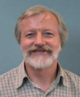
Dr. Christian Schlünder, Infineon Technologies AG
Prof. Tibor Grasser, Technische Universität Wien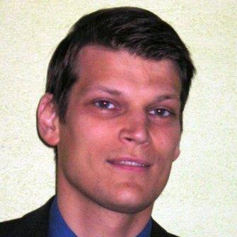
Since 1997 he has headed the Minimos-NT development group, working on
the successor of the highly successful MiniMOS program. From 2003 till
2010 he was the director of the Christian Doppler Laboratory for TCAD
in Microelectronics. Prof. Grasser is the co-author or author of over
450 articles in scientific books, journals, and conferences
proceedings, and has presented invited talks, tutorials and short
courses at various conferences such as the IEDM, IRPS, VLSI Symp.,
SISPAD, ESSDERC, IIRW, ESREF, INFOS, ISDRS, and the ECS meetings. He
is an IEEE Fellow, the editor of a book on advanced device simulation,
organic electronics, the bias temperature instability, and hot carrier
degradation, a distinguished lecturer of the IEEE Electron Devices
Society, has been involved in the program and management committees of
conferences such as IEDM, IRPS, SISPAD, IWCE, ESSDERC, IIRW, and
ISDRS, and is a recipient of the Best Paper Awards at IRPS (2008,
2010, and 2012), ESREF 2008, and IPFA (2013 and 2014) as well as the
IEEE EDS Paul Rappaport Award 2011. He was also a Chairman of SISPAD
2007 and General Chair of IIRW 2014. His current scientific interests
include semiconductor device reliability issues as well as device
modeling and simulation in general.


